Primary Capability
HDI PCB
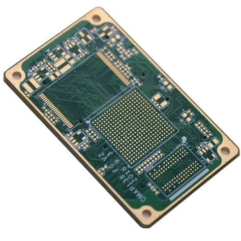
High-Density Interconnect boards use laser-drilled microvias and fine-pitch traces to pack more routing into less board area.
Overview
High-Density Interconnect boards use laser-drilled microvias and fine-pitch traces to pack more routing into less board area.
Why it matters
As components shrink and pin counts rise, standard drilling and trace widths run out of room. HDI routes fine-pitch BGAs and dense connectors without expanding the board footprint.
Typical Applications
- Smartphones and wearables
- Compact medical devices
- High-density compute modules
- Space-constrained sensor packages
Manufacturing Considerations
- Microvia aspect ratios and stacking (via-in-pad, stacked vias) affect both cost and reliability
- Fine-pitch traces require tighter process control during etching
- Sequential lamination adds manufacturing steps compared to a single-press multilayer board
Technical Characteristics
| Max layer count | Pending specification |
|---|---|
| Min trace / space | Pending specification |
| Min hole size | Pending specification |
| Standard materials | Pending specification |
| Surface finish options | Pending specification |
| Typical turnaround | Pending specification |
Exact specifications are confirmed per order -- send a spec through Request a Quote for a firm answer.
Ready to spec an HDI PCB?
Board type, quantity, layers, material -- engineering reviews the full picture.