
Products
Prototype PCB
Fast-turn boards built to validate a design before committing to a full production run.
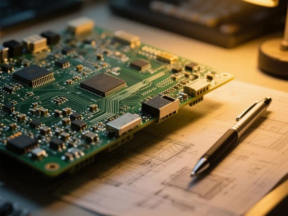
Overview
Fast-turn boards built to validate a design before committing to a full production run.
Why it matters
Catching a routing or footprint error on a five-piece prototype costs far less than catching it after a production order ships.
Typical Applications
- Design validation ahead of production
- Engineering sample builds
- Iterative hardware development
- Low-volume specialty runs
Manufacturing Considerations
- Turnaround is usually prioritized over unit cost
- Prototype-stage process should still match production intent, or validation doesn't tell you much
- Small batch sizes affect panelization and setup cost per board
Technical Characteristics
- Max layer count
- 120 layers
- Min trace / space
- 2.2 / 2.2 mil
- Min hole size
- 0.1 mm
- Standard materials
- 370HRS1000-2IT180AEM825
- Surface finish options
- HASL (Hot Air Solder Leveling)ENIG (Electroless Nickel Immersion Gold)Immersion TinOSP (Organic Solderability Preservative)Immersion SilverGold FingerElectroplated Hard GoldSelective OSPENEPIG
- Typical turnaround
- 5–7 working days
Exact specifications are confirmed per order — send a spec through Request a Quote for a firm answer. Company-wide process limits are published on the Capabilities page.
Ready to spec a Prototype PCB?
Board type, quantity, layers, material — engineering reviews the full picture.