
PCB Fabrication & Assembly
Fabrication of bare boards across every technology in the Stech range -- from conventional rigid boards to HDI, rigid-flex and metal core -- with assembly available to deliver populated boards.
Overview
Fabrication of bare boards across every technology in the Stech range -- from conventional rigid boards to HDI, rigid-flex and metal core -- with assembly available to deliver populated boards.
Why it matters
Keeping fabrication and assembly with one manufacturer removes a hand-off between suppliers, and the questions about the board get answered by the people who built it.
What's Included
- 01
PCB fabrication
High layer count, HDI, rigid, substrate-like, copper inlay, flexible, metal core, RF / high-frequency and rigid-flex boards, among others.
- 02
High layer count and fine-line builds
Up to 100 layers, HDI structures up to 8+N+8, and inner-layer line / space down to 1.7 / 1.7 mil.
- 03
Advanced processes
Back-drilling, copper fill, skip-vias, embedded capacitors and resistors, and copper coin technology.
- 04
PCB assembly
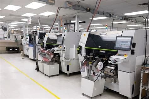
SMT, through-hole and mixed-technology assembly, single- or double-sided, so you receive populated boards rather than bare ones.
- 05
Certified quality systems
Built under ISO 9001 and IATF 16949 quality management, UL certification, and IPC Class 2/3 workmanship.
PCB Assembly Capabilities
| Assembly types | SMT, through-hole (THT) and mixed technology |
|---|---|
| Board sides | Single- and double-sided assembly |
| Smallest passive components | 01005 (0402 metric) |
| Fine-pitch packages | BGA and QFN down to 0.35 mm pitch, with X-ray inspection |
| Board size | Up to 460 × 500 mm; boards under 70 × 70 mm assembled in panels |
| Order quantity | No minimum; 1-piece prototypes through volume production |
| Soldering | Lead-free (RoHS) and leaded |
| Workmanship standard | IPC-A-610 Class 2 and Class 3 |
| Component supply | Full turnkey, consigned or partially consigned |
Inspection & Testing
- 01
Solder paste inspection (SPI)
Paste deposits are measured before placement, catching print defects before they become solder joints.
- 02
Automated optical inspection (AOI)
Placement, polarity and solder joints are checked optically after reflow.
- 03
X-ray inspection
Hidden joints under BGAs, QFNs and other bottom-terminated packages are inspected by X-ray.
- 04
In-circuit test (ICT)
Shorts, opens and component values are checked on the assembled board.
- 05
Functional test
Boards are powered and exercised to your test procedure to confirm they work as intended.
Additional Services
- 01
Conformal coating
Protective coating for assemblies exposed to moisture, dust, chemicals or temperature cycling.
- 02
Box build
Assembled boards integrated into enclosures and final assemblies, ready to ship as finished units.
Typical Lead Times
| Prototype PCB fabrication | 5–7 working days |
|---|---|
| Standard / multilayer PCB fabrication | 5–10 working days |
| HDI PCB fabricationHigher-order HDI structures take longer | 10–20 working days |
| High layer count and advanced buildsQuoted per design | 15+ working days |
| PCB assembly (boards and parts in hand) | 5–10 working days |
Typical ranges. Your actual lead time is confirmed with the quote and depends on design complexity, quantity and component availability.
How to Get Started
- 1Send Gerbers, your stack-up and a BOM (for assembly) through Request a Quote.
- 2Specify board type, quantity, layer count and material in the form.
- 3Engineering reviews the package and follows up by email.
Capabilities Behind This Service
Related Products
Start with PCB Fabrication & Assembly
Send your design data and requirements -- engineering reviews the full picture and follows up.