
Products
Copper Inlay PCB
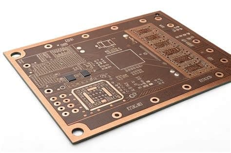
Boards with solid copper pieces -- coins or inlays -- embedded in the stack-up beneath hot components, giving heat a direct, low-resistance path out of the board.
Overview
Boards with solid copper pieces -- coins or inlays -- embedded in the stack-up beneath hot components, giving heat a direct, low-resistance path out of the board.
Why it matters
Power devices and RF amplifiers can generate more heat than thermal vias alone can remove. An embedded copper coin moves heat straight from the component to a heatsink or chassis, keeping junction temperatures down.
Typical Applications
- RF power amplifiers
- Power conversion and motor drives
- High-power LED modules
- Automotive power electronics
Manufacturing Considerations
- Inlay size and position must be fixed early -- they shape the stack-up and lamination
- Inlay surface flatness matters for component and heatsink contact
- Combining inlays with fine-pitch routing needs careful co-design
Technical Characteristics
| Max layer count | Pending specification |
|---|---|
| Min trace / space | Pending specification |
| Min hole size | Pending specification |
| Standard materials | Pending specification |
| Surface finish options | Pending specification |
| Typical turnaround | Pending specification |
Exact specifications are confirmed per order -- send a spec through Request a Quote for a firm answer. Company-wide process limits are published on the Manufacturing Capabilities page.
Ready to spec a Copper Inlay PCB?
Board type, quantity, layers, material -- engineering reviews the full picture.