
Engineering & Design Service
Schematic capture and PCB layout design through to manufacturing-ready files, plus engineering support on stack-up, materials and impedance -- so the board that gets fabricated is the board you intended.
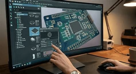
Overview
Schematic capture and PCB layout design through to manufacturing-ready files, plus engineering support on stack-up, materials and impedance -- so the board that gets fabricated is the board you intended.
Why it matters
Most fabrication problems are cheaper to solve in the design data than on the production floor. A layout drawn by the team that also fabricates the board is built around real process limits from the first trace, which avoids respins -- especially on high layer count, HDI and high-speed designs.
What's Included
- 01
Schematic capture
Schematics drawn from your requirements, block diagrams or reference designs, ready to carry straight into layout.
- 02
PCB layout design
Complete board layout from the schematic -- placement, routing, stack-up and a full manufacturing file package.
- 03
Design for manufacturability review
Design data is checked against fabrication process limits -- trace geometry, hole sizes, aspect ratio -- and issues are raised before production, not after.
- 04
Stack-up and material selection
Choosing laminates across the range Stech works with -- FR4 High Tg, Rogers 4350 / 4003, and medium- to ultra-low-loss materials -- to balance electrical performance and cost.
- 05
Controlled impedance
Impedance targets engineered into the stack-up and held to ±5%.
- 06
Signal integrity measurement
Insertion loss measurement using SET2DIL, Delta L and VNA methods for high-speed designs.
- 07
Advanced constructions
Support for HDI structures up to 8+N+8, layer counts up to 100, back-drilling, embedded components and copper coin designs.
PCB Layout Design
Layouts are drawn around Stech's own fabrication process limits, so the design that leaves layout is one the factory can build as drawn.
- 01
Component placement
Placement planned around the board outline, connectors and enclosure, signal flow, thermal paths and assembly access.
- 02
Stack-up definition
Layer count, laminate and copper weights set up front, with controlled-impedance structures held to ±5%.
- 03
High-speed and controlled-impedance routing
Differential pairs, length matching and impedance-controlled traces for high-speed interfaces, with back-drilling where via stubs matter.
- 04
HDI and fine-pitch layouts
Microvia structures up to 8+N+8 and inner-layer line / space down to 1.7 / 1.7 mil for dense BGA breakout.
- 05
RF and high-frequency layouts
Layouts on Rogers 4350 / 4003 and low-loss laminates for RF and high-frequency circuits.
- 06
Power and thermal design
Power planes and copper sized for current, with copper coin and metal core options where heat has to leave the board fast.
- 07
Every Stech board type
Rigid, flexible, rigid-flex, metal core, copper inlay and high layer count boards.
- 08
DFM built in
Design rules come from the fabrication line itself, and every layout is checked for manufacturability before release.
How a Layout Project Runs
- 01
Design inputs
You share the schematic -- or your requirements, if we're drawing it -- plus the BOM, board outline and any mechanical or electrical constraints.
- 02
Stack-up and design rules
Layer count, materials, impedance targets and design rules are agreed before layout starts.
- 03
Placement review
Component placement is reviewed with you before routing begins.
- 04
Routing
Critical nets -- high-speed, RF and power -- are routed first, then the rest of the board.
- 05
Checks and your review
Design-rule and manufacturability checks against Stech process limits, then your final review.
- 06
Release
The manufacturing file package is released, and the board can go straight into fabrication.
What to Send
- Schematic (PDF and native files) or netlist -- or your requirements, if we're drawing the schematic
- Bill of materials with manufacturer part numbers
- Board outline or mechanical drawing (DXF / STEP)
- Target layer count or stack-up, if known
- Critical requirements -- impedance, high-speed interfaces, current, thermal
- Connector, mounting-hole and enclosure constraints
What You Receive
- Gerber or ODB++ fabrication files
- NC drill files
- Stack-up and fabrication drawing
- Assembly drawing
- Pick-and-place (centroid) file
- Final bill of materials
Design Tools & Files
| EDA software | Industry-standard tools, including Altium Designer, Cadence Allegro / OrCAD and Siemens PADS / Xpedition |
|---|---|
| Manufacturing outputs | Gerber or ODB++, drill files, drawings, pick-and-place and BOM |
| Native design files | Handed over subject to the project terms |
Typical Lead Times
| PCB layout -- simple (1–4 layers) | 5–10 working days |
|---|---|
| PCB layout -- multilayer, high-speed or HDIDepends on component count, interfaces and review cycles | 3–8 weeks |
Typical ranges. Your actual lead time is confirmed with the quote and depends on design complexity, quantity and component availability.
How to Get Started
- 1Send your schematic (or requirements, if you need it drawn), BOM and board outline through Request a Quote -- or existing Gerbers for a design review.
- 2Tell us whether you need a full layout or engineering input on stack-up, materials, impedance or manufacturability.
- 3Engineering reviews the data and follows up by email with scope and timing.
Details pending confirmation
- Turnaround for a stand-alone engineering (DFM) review
Ask engineering for specifics on your project in the meantime.
Capabilities Behind This Service
Related Products
Start with Engineering & Design Service
Send your design data and requirements -- engineering reviews the full picture and follows up.