Products
High-Frequency PCB
Boards built on controlled-impedance substrates for RF, microwave, and high-speed digital signal paths.
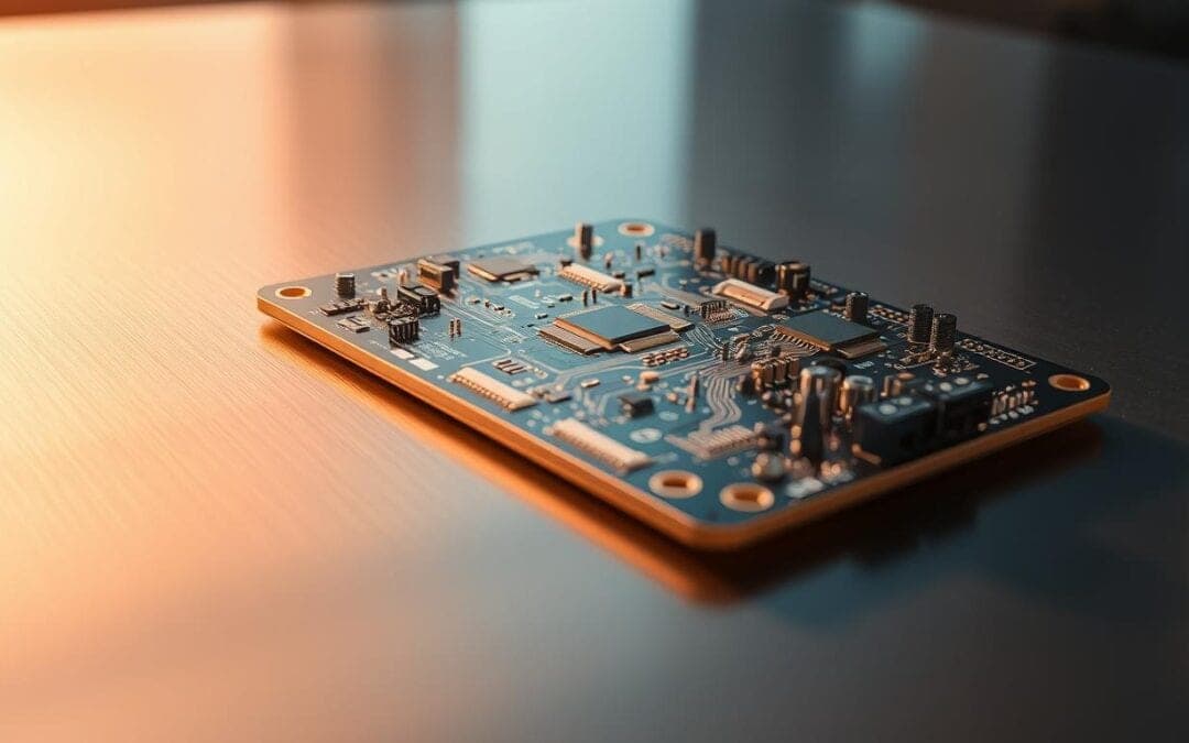
Overview
Boards built on controlled-impedance substrates for RF, microwave, and high-speed digital signal paths.
Why it matters
Above certain frequencies, standard FR-4 dielectric behavior and routing tolerances introduce signal loss and reflection. High-frequency materials and controlled trace geometry keep signal integrity intact.
Typical Applications
- RF front-ends and antennas
- Radar and communications equipment
- High-speed digital interfaces
- Test and measurement instrumentation
Manufacturing Considerations
- Dielectric constant stability across frequency and temperature matters as much as the base material choice
- Trace geometry and reference planes must be controlled together to hit a target impedance
- Connector and via transitions are common sources of signal degradation if not modeled
Technical Characteristics
| Max layer count | Pending specification |
|---|---|
| Min trace / space | Pending specification |
| Min hole size | Pending specification |
| Standard materials | Pending specification |
| Surface finish options | Pending specification |
| Typical turnaround | Pending specification |
Exact specifications are confirmed per order -- send a spec through Request a Quote for a firm answer.
Ready to spec a High-Frequency PCB?
Board type, quantity, layers, material -- engineering reviews the full picture.