Primary Capability
High-Complexity PCB
Advanced builds that combine multiple demanding requirements at once -- high layer counts, fine features, mixed materials, or unusual mechanical constraints.
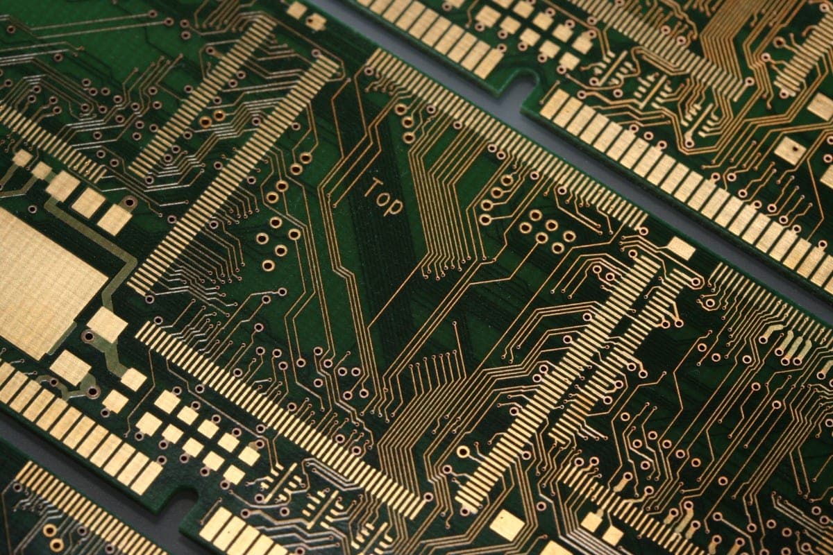
Overview
Advanced builds that combine multiple demanding requirements at once -- high layer counts, fine features, mixed materials, or unusual mechanical constraints.
Why it matters
Some designs don't fit neatly into one category. A board might need HDI routing density, high-frequency performance, and high-Tg thermal stability at the same time.
Typical Applications
- Advanced compute and networking hardware
- Aerospace and defense electronics
- Multi-technology sensor and RF modules
- Designs pushing past a single fabrication category
Manufacturing Considerations
- Combining technologies compounds process complexity, not just cost
- Design-for-manufacture review matters more here than on any single-technology board
- Engineering collaboration early in the design cycle reduces late-stage surprises
Technical Characteristics
| Max layer count | Pending specification |
|---|---|
| Min trace / space | Pending specification |
| Min hole size | Pending specification |
| Standard materials | Pending specification |
| Surface finish options | Pending specification |
| Typical turnaround | Pending specification |
Exact specifications are confirmed per order -- send a spec through Request a Quote for a firm answer.
Ready to spec a High-Complexity PCB?
Board type, quantity, layers, material -- engineering reviews the full picture.