Primary Capability
Multilayer PCB
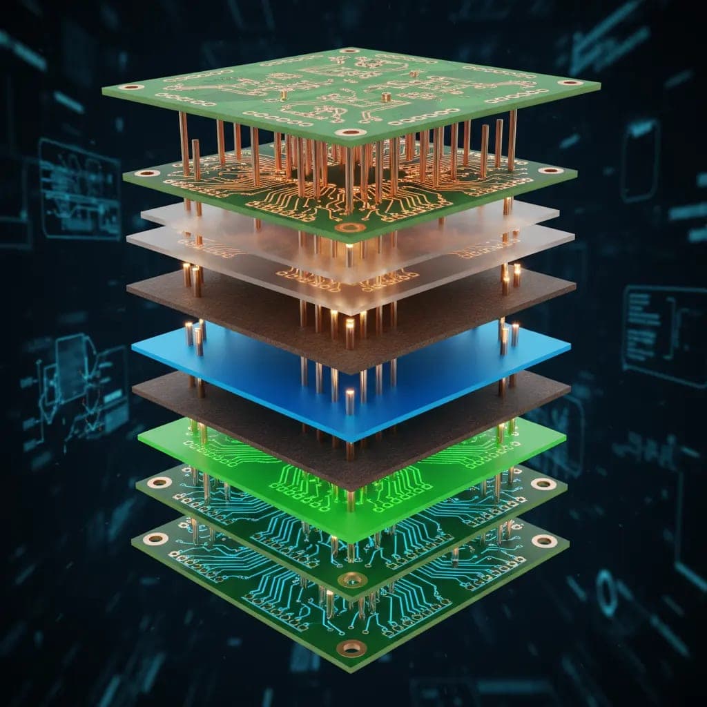
Three or more conductive layers laminated together, separating power, ground, and signal routing across dedicated planes.
Overview
Three or more conductive layers laminated together, separating power, ground, and signal routing across dedicated planes.
Why it matters
Dense designs need more routing area than a single board surface can provide, and dedicated ground and power planes improve signal integrity and reduce noise.
Typical Applications
- Industrial control systems
- Compute and networking hardware
- Automotive electronic control units
- Dense mixed-signal designs
Manufacturing Considerations
- Layer stack-up sequencing affects impedance control and manufacturability
- More layers generally mean tighter lamination tolerances
- Via structures -- through, blind, buried -- need to be planned alongside the stack-up, not after
Technical Characteristics
| Max layer count | Pending specification |
|---|---|
| Min trace / space | Pending specification |
| Min hole size | Pending specification |
| Standard materials | Pending specification |
| Surface finish options | Pending specification |
| Typical turnaround | Pending specification |
Exact specifications are confirmed per order -- send a spec through Request a Quote for a firm answer.
Ready to spec a Multilayer PCB?
Board type, quantity, layers, material -- engineering reviews the full picture.