
Products
Burn-in Board
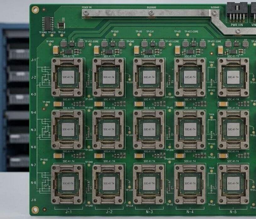
Boards that carry semiconductor devices through burn-in -- extended operation at elevated temperature and voltage -- so early-life failures are screened out before parts ship.
Overview
Boards that carry semiconductor devices through burn-in -- extended operation at elevated temperature and voltage -- so early-life failures are screened out before parts ship.
Why it matters
A burn-in board spends long periods in an oven with many devices loaded at once. Laminate, plating and finish have to withstand sustained heat and repeated socket insertions without warping or losing contact.
Typical Applications
- Semiconductor reliability screening
- Burn-in and high-temperature operating life (HTOL) test
- Memory and logic device qualification
- Automotive-grade component screening
Manufacturing Considerations
- High-temperature laminates such as polyimide or high-temp FR4 resist warping over long oven cycles
- Hard-gold contact areas stand up to repeated socket insertions
- Power distribution has to feed many devices at once without excessive voltage drop
Technical Characteristics
- Max layer count
- 38 layers
- Min trace / space
- 2.5 / 2.5 mil
- Min hole size
- 0.1 mm
- Standard materials
- Polyimide / High Temp FR4
- Surface finish options
- ENIGENEPIGSelective Hard Gold / Soft Gold
- Typical turnaround
- 15+ working days, quoted per design
Exact specifications are confirmed per order -- send a spec through Request a Quote for a firm answer. Company-wide process limits are published on the Manufacturing Capabilities page.
Ready to spec a Burn-in Board?
Board type, quantity, layers, material -- engineering reviews the full picture.