
Products
Probe Card
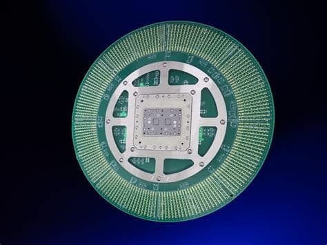
The multilayer PCB at the heart of a wafer probe card -- it routes signals between the tester and the probe head that contacts each die on the wafer.
Overview
The multilayer PCB at the heart of a wafer probe card -- it routes signals between the tester and the probe head that contacts each die on the wafer.
Why it matters
A probe card concentrates a very large number of signals into the small area around the probe head. That takes high layer counts, fine line and space, and low-loss materials, with flatness and plating quality held tightly across the board.
Typical Applications
- Wafer sort and wafer-level test
- Semiconductor device characterization
- High-speed and RF device test
- Memory and logic wafer test
Manufacturing Considerations
- Dense signal fan-out around the probe head drives layer count and line / space
- Low-loss laminates such as Megtron keep high-speed test signals clean
- Flatness and gold contact areas matter where the board meets the probe head and the tester
Technical Characteristics
- Max layer count
- 52 layers
- Min trace / space
- 2.5 / 2.5 mil
- Min hole size
- 0.1 mm
- Standard materials
- PolyimideM6GMegtronIsola
- Surface finish options
- ENIGENEPIGSelective Hard Gold / Soft Gold
- Typical turnaround
- 15+ working days, quoted per design
Exact specifications are confirmed per order -- send a spec through Request a Quote for a firm answer. Company-wide process limits are published on the Manufacturing Capabilities page.
Ready to spec a Probe Card?
Board type, quantity, layers, material -- engineering reviews the full picture.